
Atomic-layer additive manufacturing enables ultrathin antimony sulfide photovoltaics with nanometer precision
Fabricating ultrathin solar cells efficiently requires precise control at the nanometer scale. Atomic layer deposition (ALD) provides excellent control over film thickness, but conventionally coats the entire substrate, requiring additional patterning steps to define device structures. Atomic-layer additive manufacturing (ALAM) overcomes this limitation by combining the chemical precision of ALD with the flexibility of 3D printing. Using a microfluidic nozzle to confine deposition to selected areas, ALAM enables direct patterning of materials and device architectures on the substrate. This approach allows rapid prototyping of multiple device designs in a single process, reduces material consumption, and eliminates the need for separate lithographic steps, making it particularly well suited for exploring and optimizing ultrathin photovoltaic structures.
In a new study, CorMic doctoral researcher Micah Mc Naire and colleagues from Friedrich-Alexander-Universität Erlangen-Nürnberg (FAU), together with partners from Ruhr University Bochum, the Leibniz Institute for Solid State and Materials Research Dresden and TU Dresden, applied this approach to ultrathin inorganic solar cells. The work has been published in the Nature Portfolio journal Communications Materials.
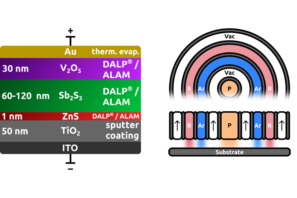
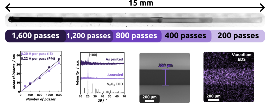
The researchers developed ALAM processes for the three central semiconductor layers: zinc sulfide (ZnS), antimony sulfide (Sb2S3) and vanadium oxide (V2O5), demonstrating the high flexibility of the technique in integrating different material classes within a single fabrication approach. All three materials exhibited true ALD-type growth behavior, with controlled layer-by-layer deposition and thickness precision comparable to conventional ALD. The resulting films were characterized by smooth surfaces, high compositional purity and, after annealing, crystalline structures. This well-defined growth and structural quality provide an ideal platform for correlative microscopy, enabling detailed investigations of how nanoscale morphology and interfaces influence device performance.
A particularly important finding concerned the interface underneath the Sb2S3 light absorber. Without an intermediate layer, the absorber formed discontinuous films and dewetted during crystallization. Adding an approximately one-nanometer-thick ZnS layer stabilized the Sb2S3 and produced a continuous, crystalline film with a surface roughness below one nanometer. This demonstrates how interfaces only a few atomic layers thick can determine the structure of an ultrathin photovoltaic device.
The printed ZnS/ Sb2S3/ V2O5 stack was subsequently combined with titanium dioxide, transparent indium tin oxide and gold contacts. The resulting devices generated measurable photocurrent and photovoltage under illumination. Crucially, this work represents the first demonstration of fully inorganic solar cells fabricated in a single, continuous ALD-based additive manufacturing process with direct patterning, eliminating the need for separate lithography or masking steps. This demonstrates a novel fabrication approach, where complete photovoltaic architectures can be built layer by layer with nanometer precision in one integrated process. The current devices are a proof of concept and still exhibit low power conversion efficiencies, limited charge transport, and non-ideal interfaces that lead to recombination losses, as well as challenges in long-term stability and scalability.
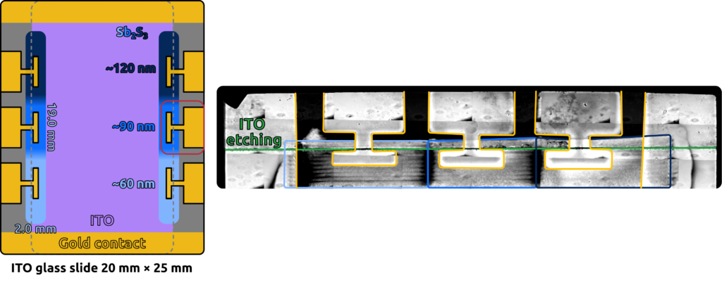
At the same time, ALAM provides a powerful platform to address these limitations through rapid and material-efficient optimization. Different absorber thicknesses, layer sequences and device geometries can be produced and directly patterned on the same substrate within a single deposition run, enabling systematic studies with minimal material consumption, with precursor use reduced by at least a factor of 1,000 compared with an equivalent chamber-based ALD investigation.
The work connects directly with CorMic project A4, which investigates how interfaces, processing conditions and nanoscale morphology influence atomic-layer-processed thin-film solar cells. Combining ALAM with correlative microscopy and functional characterization will help establish relationships between fabrication, material structure and photovoltaic performance.